Wafer cleaning issues at the wet process
Model of the failure:
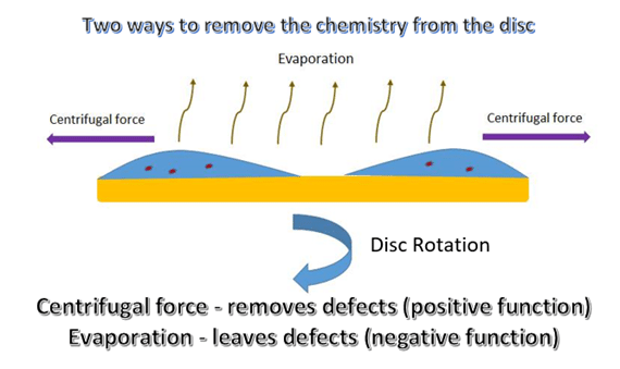
The chemistry evaporates too fast, therefore particles remain on the
Short term solution:
Reduce the evaporation rate of the chemistry (water at rinsing)
- Increase air pressure above the wafer
- Reduce the temperature of the chemistry
- Adjust the flow of the chemistry and rotation rate of the wafer to keep the chemistry on the wafer during the process. Keep in mind that the flow increases the amount of chemistry while wafer rotation removes the chemistry from the wafer

Long term solution
Use a shower (multiple nozzles system) instead of a single movable nozzle. The flow should be adjustable above different areas of the wafer.
Shower:
Multy-nozzles system:
Adjust recipe for no "empty" areas on the wafer during the process
Similar projects
The process is related to microelectronics - microchip manufacturing. The purpose of the process is to create a SiO2 layer on the surface of a Si wafer. Equipment: Vertical furnace to heat the wafers in the Q2 atmosphere and perform oxidation on the wafer surface. Process: The oxidation occurs on the front side and on the back side of the wafer Requirements: Create a SiO2 thin layer with a certain thickness and low sigma - low standard deviation of the thickness between the wafers and within the wafer Failure: Wafers from the lower zone have higher thickness and significantly higher within wafer sigma (standard deviation of the thickness within the wafer)
Semiconductor devices are becoming more complex and expensive. But what exactly are we paying for when we buy a computer, cellphone, or any device containing a microchip? It’s not for radically new functions—the core components remain the same: transistors and interconnections. According to Moore’s law, transistors are getting smaller, with more interconnection layers added, making the manufacturing process longer and more costly. In reality, we’re paying for the inability of engineers to efficiently solve engineering challenges. This project leverages System Functional Modeling (SFM) to analyze the IC interconnection layer and Process Functional Modeling (PFM) to evaluate its manufacturing process. These analyses aim to deepen our understanding of both the device and the production process, generating innovative solutions for cost reduction and improved efficiency.
The project was dedicated to production yield improvement in microchip manufacturing. The bumps are created on the top of a wafer and used for the final test of all dies. Only good dies are taken for the packaging. All dies that fail the test will be scrapped. The process yield depends on the amount of "good" and "bad" dies. It was revealed that in some cases, the time between the end of the process and the final test impacts the yield. The longer the dwelling, the more dies fail the final test. If the dwelling exceeds hundreds of hours, the amount of failed dies becomes dramatically high, which results in the scrapping of the whole wafer. The problem was analyzed and solved.