
Here's what's popular on Priz.guru

Wet cleaning is widely used in microchip manufacturing. Single wafer equipment is working as follows. A wafer rotates, and chemistry is poured from a movable nozzle. Water rinsing is performed at the end of the process. Loading of a new batch of the chemistry resulted in excursion - a strongly increased amount of defects was observed on the wafer after the processing. The project is dedicated to the failure analysis and creation of innovative solutions.

Flash heating of a wafer is widely used in microchip manufacturing. The purpose of the process is to prevent the diffusion of ions and atoms. During the flash process, a wafer breakage occurs. The project's purpose is to learn and understand the mechanism of the wafer breakage and propose the solutions to prevent the wafer breakage

The process is related to microelectronics - microchip manufacturing. The purpose of the process is to create a SiO2 layer on the surface of a Si wafer. Equipment: Vertical furnace to heat the wafers in the Q2 atmosphere and perform oxidation on the wafer surface. Process: The oxidation occurs on the front side and on the back side of the wafer Requirements: Create a SiO2 thin layer with a certain thickness and low sigma - low standard deviation of the thickness between the wafers and within the wafer Failure: Wafers from the lower zone have higher thickness and significantly higher within wafer sigma (standard deviation of the thickness within the wafer)
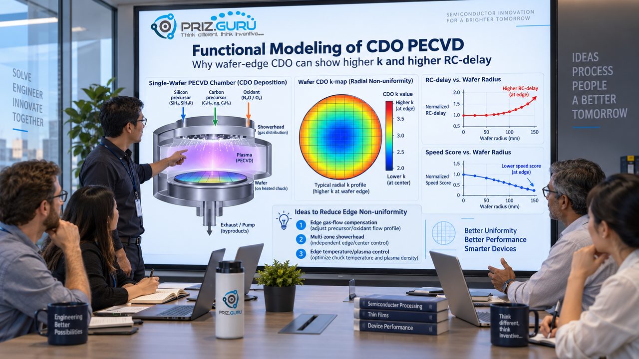
This project investigates radial non-uniformity of CDO low-k dielectric deposited by PECVD and its possible impact on wafer performance. Final test data indicate that faster dies are mainly located closer to the wafer center, while slower dies are more often found near the wafer periphery. The corresponding RC-delay trend also increases toward the wafer edge. The focus of the project is the capacitance component of RC-delay. CDO is expected to provide a low dielectric constant between BEOL metal lines, but the deposited film may not have uniform properties across the wafer. Near the wafer edge, the process can be influenced by different gas flow, plasma behavior, residence time, temperature, and pumping conditions. This may lead to stronger oxidation and deeper precursor decomposition near the periphery, forming CDO that is more oxygen-rich, less carbon-rich, denser, and closer in behavior to SiO₂. As a result, the dielectric constant k may increase toward the wafer edge, causing higher interline capacitance, higher RC-delay, and lower die speed. The project uses Functional Modeling to understand how PECVD chamber components and process conditions affect CDO film properties. The goal is to identify the main functional and problematic interactions and propose directions for compensation, such as radial gas-flow tuning, multi-zone showerhead design, edge compensation flow, and local plasma or temperature control.
Work on your own project, solve tough problems & share creative solutions
Publish your projects on PrizHub and remove all the limitations on a Free Plan. Promote yourself and your team in the community, involve investors, followers and contributors.

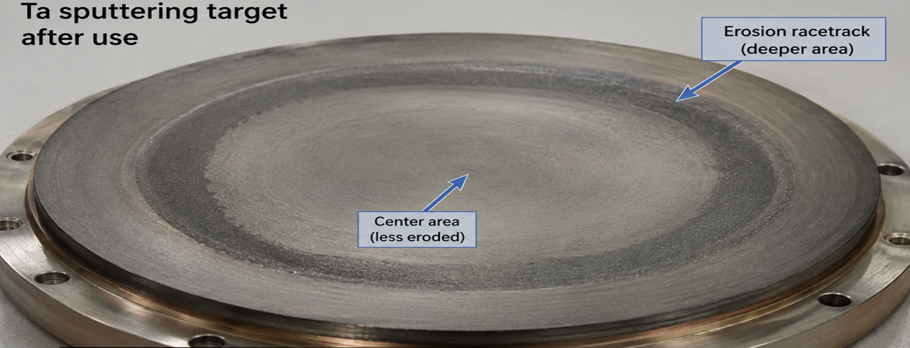
This project investigates the nonuniform erosion of an expensive Ta sputtering target during Ta/TaN PVD. A deep racetrack groove forces target replacement while a significant amount of tantalum remains unused. Using PRIZ problem-solving tools, the project explores the system’s functions, identifies the root causes of localized erosion, and develops ways to improve target utilization without reducing deposition rate or production throughput.