
Found 12 projects in Microelectronics
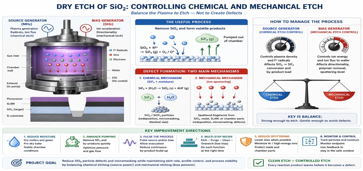
This project investigates particle-defect formation during SiO₂ dry etch. Functional modeling revealed that defects can be generated by two coupled mechanisms: chemical formation of SiO₂/SiOFₓ particles from SiF₄ interaction with moisture, and mechanical generation of particles by excessive ion bombardment and sputtering. The proposed improvement direction is to balance chemical etching and ion-assisted etching by properly adjusting the source and bias generators, reducing moisture, improving by-product evacuation, minimizing sputtering, and using pulsed or multi-step process recipes. The goal is to reduce particles and micromasking while maintaining etch rate, profile control, and process stability.
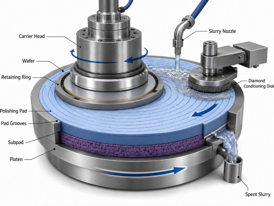
This project investigates how to increase the copper removal rate during Chemical Mechanical Planarization (CMP). Functional modeling revealed that increasing H₂O₂ alone is ineffective beyond an optimum level because rapid oxidation creates a thick, passivating Cu₂O/CuO layer that must be mechanically removed. The winning direction is to balance faster oxidation with stronger mechanical removal by optimizing pad speed, abrasive concentration, pressure, conditioning, and slurry transport.

Semiconductor devices are becoming more complex and expensive. But what exactly are we paying for when we buy a computer, cellphone, or any device containing a microchip? It’s not for radically new functions—the core components remain the same: transistors and interconnections. According to Moore’s law, transistors are getting smaller, with more interconnection layers added, making the manufacturing process longer and more costly. In reality, we’re paying for the inability of engineers to efficiently solve engineering challenges. This project leverages System Functional Modeling (SFM) to analyze the IC interconnection layer and Process Functional Modeling (PFM) to evaluate its manufacturing process. These analyses aim to deepen our understanding of both the device and the production process, generating innovative solutions for cost reduction and improved efficiency.

Flash heating of a wafer is widely used in microchip manufacturing. The purpose of the process is to prevent the diffusion of ions and atoms. During the flash process, a wafer breakage occurs. The project's purpose is to learn and understand the mechanism of the wafer breakage and propose the solutions to prevent the wafer breakage
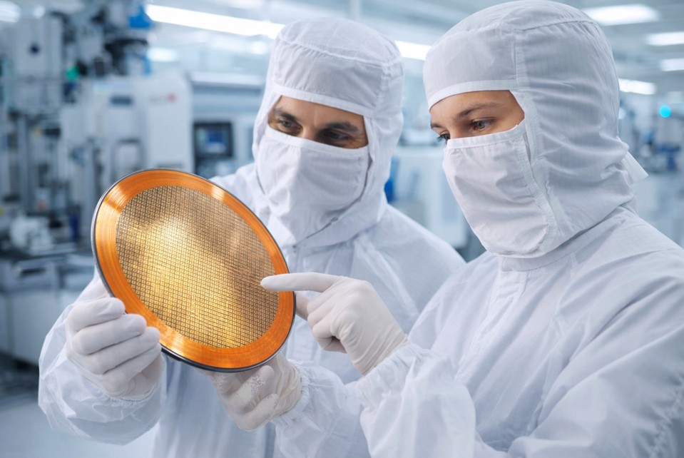
Copper electroplating is essential for forming advanced semiconductor interconnects, yet radial thickness non-uniformity remains a costly challenge. Thicker deposition at the wafer edge and thinner copper at the center force manufacturers to rely on overplating and CMP compensation, increasing material waste and process cost. Using the PRIZ Platform, this project reveals that the true amplification mechanism lies in operating within a kinetically controlled regime, where small voltage variations caused by seed-layer resistance produce large thickness deviations. By shifting the process closer to diffusion-controlled behavior and reducing sensitivity to voltage fluctuations, uniform deposition can be achieved intrinsically — enabling thinner seed layers, reduced overplating, lower CMP burden, and overall cost reduction.